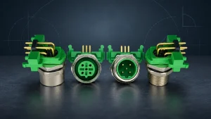
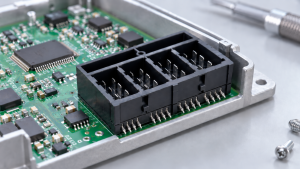
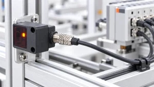
During layout review, a 2.54 mm, ten-position header sits 3 mm from the enclosure wall. The footprint matches the schematic and the BOM part number. Cable seating fails because exit direction never entered the lid check before layout release. A right-angle version from the same series may solve the fit issue without a major redesign, but cost still depends on material, plating, MOQ, and supplier quotation. By then, the board has already lost two review cycles.
Board connection comes first. Low level signals, power rails, ground returns, service access, and factory programming each push different limits for current rating, voltage margin, mating direction, soldering process, and clearance around the finished assembly. Those limits narrow pin count, pitch, row count, mounting style, and plating before the part number search begins.
Build the shortlist from the board requirement list before opening the catalogue. Define connection role, current, voltage, mating direction, soldering process, and service access first. Then apply pitch, row count, mounting style, orientation, and plating as filters on the pin header connector options page.
Specify the Pin Header Connector's PCB Role First
Two headers share a 2.54 mm, ten-position footprint in the CAD library, then serve different jobs on the board. Display signals need short returns, visible pin 1 marking, and probe space. Motor driver outputs need low contact resistance, stronger retention, and grouped supply-return pins. Our PCB pin connector design guide ties the role check to pinout, marking, and probe access. The IPC design standards provide the land pattern and spacing standards behind those layout choices.
Connection path and service life reshape the shortlist. Board-to-board headers get checked by stack height and alignment tolerance. Wire-to-board headers get checked by cable exit, bend clearance, and handling room during assembly. Factory programming contacts see limited bring-up and test cycles; removable modules put plating, contact force, and housing support under repeated wear. After the PCB job is clear, pitch, pin count, row structure, mounting style, and finish have a concrete reason behind them.

Choose Pitch, Pin Count, and Row Structure
Start the pin-count estimate by adding ground returns and spare positions to the required signal and power pins. During layout review, adjust that count for current sharing, signal return paths, creepage and clearance, reserved-pin strategy, and assembly tolerance. Then measure the available board edge, compare usable pitch options, and shortlist the connector size. Row count comes last, after escape routing is confirmed under the connector.
Smaller pitch buys board edge and spends routing margin. Moving from 2.54 mm to 2.00 mm shortens the header by roughly one fifth, and dual row cuts length again. The trade moves into creepage, clearance, escape routing, extra layers, or narrower traces.
Our pin header product range lets engineers filter by pitch, row count, mounting type, rated current, orientation, and plating, with 2.54 mm, 2.0 mm, and 1.27 mm among the listed pitch options. For example, the official page for the 2.0mm Pitch Dual Row 2×5 Pin 90 Degree Pin Header Connector lists model number PBXXXCXXXCBXGF, a 1.5 Amps current rating, and Withstanding Voltage AC 500Vmin/Minute. Soulin treats those figures as datasheet limits for derating, energized-contact count, and final-board footprint review. Checking stock, MOQ, drawing revision, and mating-part availability before drawing the footprint helps prevent another layout pass.
Table 1. Pin Header Connector Pitch and Row Structure Selection Guide
| PCB condition | Selection direction | Why it matters |
|---|---|---|
| Prototype or test access | 2.54mm, single row, through hole | Easier probing, hand soldering, and field modification |
| Compact control board | 2.0mm or 1.27mm, dual row | Saves board space while keeping enough pin positions |
| Higher pin density | Dual row layout | Reduces connector length but raises routing and alignment checks |
| Simple signal header | Single row layout | Easier pin identification and lower assembly risk |
Bench validation argues against chasing the last millimeter. Headers touched by probes, clips, or hand rework during bring-up usually stay at 2.54 mm unless enclosure space forces a smaller pitch. Board edge saved by 2.00 mm disappears quickly after the first slipped probe.
Choose the Mounting Style and Connector Direction
Mounting style and connector direction need two separate checks before the catalog filter. Mounting style sets solder process and handling load. Connector direction sets the cable, daughterboard, or ribbon path after the housing closes. The article of pin header types, sizes, and applications separates straight, right angle, THT, and SMT choices along that line.
Align Mounting Style With Solder Process and Handling Load
Through-hole headers fit hand contact, cable strain, panel access, and repeated plugging. The plated barrel carries insertion force into the laminate and protects the pad during service. SMT headers fit internal stacks and high-volume boards already built through reflow, especially where low profile and assembly speed matter more than plug-and-unplug strength.
Set Connector Direction by Cable Exit and Enclosure Clearance
For example, a 2.0 mm dual-row header may stay vertical in a 25 mm instrument case when the ribbon exits through the top and nearby components leave mating room. In a 12 mm wall panel, vertical height may fail before the electrical design changes, so we move the shortlist toward a right-angle body and a cable path parallel to the PCB. For frequent plugging, we usually check through-hole right-angle bodies first because cable pull can load the solder joint in shear. The 2.0mm Pitch Dual Row 2×5 Pin 90 Degree Pin Header Connector puts a 2×5 dual-row layout in that form, with brass contacts, Au G/F over Ni plating, PA9T plastic material, Polyester (UL94V-0) insulation, and an operating temperature range from -40℃ to +105℃.

Validate Electrical Load and Contact Finish
At Soulin, we keep the pin header shortlist open until circuit checks are complete. The review covers actual current, working voltage, energized-contact count, creepage, clearance, and insulation margin before footprint approval. Tin or gold plating should match expected mating cycles, operating environment, and signal-stability requirements rather than sit as a price-only decision. The 2.0mm Pitch Dual Row 2×5 Pin 90 Degree Pin Header Connector provides current rating, insulation resistance, and contact resistance references for this review. Our gold and tin plating comparison explains how finish choice affects cost, mating life, and service reliability.
Table 2. Electrical Load and Contact Finish Selection Guide
| Parameter | Key Considerations | Selection Guideline |
|---|---|---|
| Current Rating | Load current, energized contacts, derating | Apply derating when adjacent contacts carry current simultaneously. |
| Working Voltage | Operating voltage, creepage, clearance | Verify connector spacing against insulation requirements before approving the footprint. |
| Contact Finish | Mating cycles, environment, signal integrity | Tin fits standard-duty applications; gold fits frequent mating or high-reliability signals. |
Confirm the Mating Side, Stack Height, and Pin 1 Orientation
Treat the male header as one half of the connection. Select the female header, socket, or cable assembly in the same pass because it controls footprint, stack height, assembly sequence, and service clearance.
Pair the male header with the correct female header, socket, or cable assembly
Pitch match alone does not complete the fit check. Contact style, insulator height, keying, and current rating need to match on both halves before the male header is released with its mating side. Our female header connector range includes filters for pitch, row count, pin configuration, mounting type, contact type, current rating, orientation, and plating, so engineers can keep the male and female sides within one coordinated selection path.
Set mating height around the enclosure and PCB stack
Stack height sums header height, socket height, standoff tolerance, and component keepout on both boards. Build that into the mechanical model before releasing the footprint. For wire to board, add housing depth plus bend room, often 10mm to 15mm beyond a first pass estimate.
Mark pin 1 where assembly operators see it
Silkscreen a square pad, a chamfer, and a printed numeral near the correct corner, then check it against the mating connector from the operator view. Schematic pinout still comes back reversed when the silkscreen and housing key disagree.
Apply the Selection Rules to Common PCB Scenarios
Each PCB scenario pushes one constraint to the front. Prototype access, IoT board area, industrial retention, board-to-board stack height, and test-port reach change the first filter. For industrial control boards, we do not treat gold plating or a +105C insulator as a default choice. We move them up the shortlist when the connector faces high mating cycles, vibration, humidity, heat rise, or low-level signal stability requirements. Missing that dominant constraint usually creates an enclosure, assembly, or field-service failure.
Table 3. Pin Header Connector Selection by PCB Scenario
| PCB Scenario | Recommended Selection | Failure Mode |
|---|---|---|
| Prototype board | 2.54mm single-row THT header | Excess board length in the final enclosure |
| Compact IoT or sensor board | 2.00mm or 1.27mm SMT, derating checked | Current margin loss or process rework |
| Industrial control board | Through-hole body with retention checked first. Consider gold finish and PA9T or +105°C operating-temperature-rated material for high mating cycles, vibration, humidity, heat rise, or low-level signals | Intermittent contact under vibration, humidity, repeated mating, or heat cycling |
| Board-to-board module | Matched board-to-board pair by stack height and alignment | Stack binding from tolerance or PCB warp |
| Test or programming port | Edge-access header with clear pin 1 marking | Blocked access or reversed mating |
Check the Footprint and Assembly Details Before Sampling
Before Gerbers, BOM, and assembly drawings go out, complete one physical review. Many production connector problems start as footprint or process mismatches. The PCB pin connector layout and DFM checklist lists the drill, pad, and clearance items worth re-reading here.
Table 4. PCB Header Pre-Sampling Checklist
| Check item | What to review | Risk when missed |
|---|---|---|
| Footprint | Pitch, drill size, pad size, row spacing | Connector fits the schematic but fails on the PCB |
| Direction | Straight or right angle exit | Cable or mating board conflicts with enclosure space |
| Assembly process | THT, SMT, wave, reflow, selective soldering | Part misses the planned production process |
| Mechanical clearance | Mating height, nearby parts, cable bend room | Enclosure assembly blocks connector access |
| BOM details | Pitch, pin count, row count, plating, mating part, packaging | RFQ delays or wrong-part substitution |
Common Mistakes When Selecting Pin Header Connectors
This checklist belongs before PCB footprint, enclosure model, and BOM release. Each item connects a design miss to the failure it can create and the review action we complete before sampling.
- Connector direction is added too late. Electrical testing may pass, but the cable or mating board can collide with the enclosure after layout freeze. Our review confirms straight versus right-angle direction in the mechanical model before footprint release.
- Cable exit is not measured. The cable may bind against the enclosure wall or nearby components. We verify right-angle clearance, bend radius, and service-access room from the final assembly position.
- Pin 1 view is not verified. The schematic pinout may be correct while the production line installs the mating side backward. We compare silkscreen marking, housing keying, and operator view before drawing approval.
- Plating is treated only as a cost item. Service connections may turn intermittent after repeated mating, vibration, or humidity exposure. We match tin or gold finish to mating cycles, signal level, and application environment.
- BOM details are checked after release. Stock, MOQ, packaging, or mating-connector availability can delay the build. We confirm supplier quotation, packaging format, mating part, and sample availability before PCB release.
FAQ
Conclusion
Release a pin header connector for sampling after four gates pass. First, define the connection role and electrical load. Second, confirm pitch, pin count, row count, mounting style, and orientation against board space and routing. Third, pair the female header, stack height or cable exit, plating, PCB thickness, soldering process, and operating environment. Fourth, review footprint, drawing, packaging, MOQ, stock, and sample availability before release.
We support release-stage pin header connector review by confirming the drawing, footprint, material and plating specification, current and voltage ratings, contact resistance, insulation resistance, temperature rating, packaging format, mating-part recommendation, and sample availability. Any connector option that cannot pass enclosure clearance, derating, creepage and clearance, mating height, assembly process, service access, or stock-availability checks should stay off the release list before footprint release.
For a compact, right-angle, dual-row, SMT, through-hole, or custom pin header connector, send your PCB connector requirements to Soulin with the confirmed drawing, target quantity, application environment, and release-stage constraints for part matching or custom connector support.